A NOT gate or an inverter in digital logic is one type of logic gate used to implement logical negation. The main function of this logic gate is to give an opposite bit of output to the input. So this logic gate is also known as a complement gate. Together with the OR gate & AND gate, any function within binary mathematics may be executed. This article discusses an overview of the 74HCT04 Hex Inverter, pin configuration, specifications, and its applications.
What is 74HCT04 Hex Inverter?
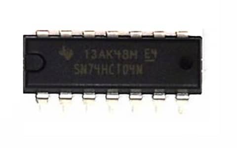
The 74HCT04 hex inverter IC includes six independent inverters by typical push-pull outputs. This IC is a high-speed inverter where these pins are compatible with low-power Schottky TTL. All the inputs of this inverter IC are simply protected from electric discharges throughout the protection network of diodes which gives safety from input voltages more than Vcc by simply allowing the utilization of resistors. This IC operates with voltage ranges from 4.5V-5.5V.

74HCT04 Hex Inverter IC
Pin Configuration:
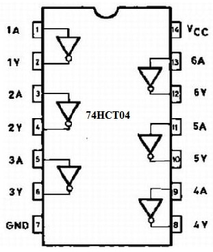
The pin configuration of the 74HCT04 hex inverter is shown below. This IC includes fourteen pins and each pin and its functionality is discussed below.

74HCT04 Hex Inverter PinOut
- Pins 1,3,5,9, 11 & 13 (Input Pins): All these pins are the Inverter ICs input pins.
- Pins 2,4,6,8, 10 & 12 (Output Pins): All these pins are the Inverter ICs output pins.
- Pin7 (Ground): It is connected to the GND of the system.
- Pin 16 (Vcc): It provides typically +5V to the inverter IC.
Features & Specifications:
The features and specifications of the 74HCT04 hex inverter include the following.
- It is a 16-pin IC and it has a standard pin configuration.
- It is also available within the SMD type.
- It is a high-speed CMOS type
- It includes six independent NOT Gates.
- It is available in different packages like SO-14, TSSOP & PDIP.
- Its operating voltage ranges from 4.5V – 5.5V.
- Its source or sink current is 4mAmp at 4.5Volts.
- Its continuous o/p current is ±25mAmps.
- Its high-level i/p voltage minimum is 2 volts.
- Its low-level i/p voltage maximum is 0.8 volts.
- Its propagation delay or transition time maximum is 29 nano sec.
- The input pins of this inverter IC have Schmitt trigger action.
- All the pins of this IC are TTL compatible.
- Equivalent 74HCT04 hex inverter ICs are; 74LS14, 74LS05, 74LS04 and CD4009. The Other logic gates are; 74LS08, 74LS00, 74LS86, and 74LS85.
Working
The 74HCT04 IC works very simply by using six inbuilt NOT gates where every gate has input & output. The input pins of this logic gate are supplied through signals. Pin 8 of this IC is connected to the GND of the circuit & pin 16 is connected to the +ve voltage supply.
Before understanding this inverter IC operation, first, we have to know the NOT gate behavior whenever applied by an input signal. The Boolean equation of NOT gate is Y = ~A, which means when the input is HIGH or 1, the output of this gate will be LOW or 0. The NOT gate truth table is given below.
The 74HCT04 inverter IC also works in the same manner. So NOT gates inside this IC have a similar truth table.
How to use 74HCT04 IC?
74HCT04 IC includes six inverting or NOT gates which work as 6 individual logic gates. This IC is very simple to use because the pins are compatible with TTL so not many external components are required. This IC works whenever the supply is given to the IC, it gives the input signal & we will obtain the o/p on the equivalent pin.

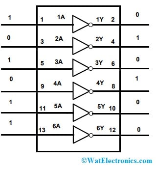
74HCT04 IC Circuit Diagram
In the above circuit, we can observe that the six logic gates in the IC operate individually depending on the i/p signal. In addition, it is also significant to keep in mind that in the simulation above, pin 14 (power pin) & pin 7 (ground pin) is not shown. Thus practically, the GND pin has to be given to GND whereas the power pin has to be supplied with +5V. The NOT gate truth table is given above where input and outputs are represented with A & Y. So we know the function of this gate which is discussed below so, this logic gate IC is known as an inverter.
The highest low-level i/p voltage of this gate is 0.8Volts, so anything above that will be believed as high & the least high-level voltage of this gate is 2V. So anything below that voltage can be considered as low. Thus this inverter IC can also function with 3.31volt signal lines to make it appropriate for a 3.3Volts to 5Volts logic level converter.
The important parameter to consider within the 74HCT04 gate inverter is switching time whenever the inverter IC works as a buffer/ wave oscillator. This IC has the capability of how speedily it toggles the o/p depending on the alteration within the input. For the o/p pin of the IC, the time taken for changing from one condition to another known as propagation delay is approximately 29nSec for this inverter IC.
Where to use 74HCT04 inverter IC/Applications?
The applications of 74HCT04 inverter IC include the following.
- 74HCT04 inverter IC is used within inverting applications.
- This IC is used to design combinational logic circuits.
- It is used to design oscillators because of their less power utilization.
- This inverter IC can be used to design square wave oscillators that deploy in producing CLK signals.
- This inverter IC works as a buffer/wave oscillator based on how rapidly it toggles the o/p on adjusting the i/p signal.
- It is used to interface NMOS or TTL o/ps to high-speed CMOS i/ps as a logic-level converter.
- It is used in designing general-purpose logic & also combinational circuits.
- It is used to handle arithmetic operations.
Issues faced While using 74HCT04 inverter IC :
While the 74HCT04 inverter IC is a commonly used and reliable component, there are a few potential issues that can be encountered when using it. Here are some common issues faced when using the 74HCT04 inverter IC:
-
Power Supply Voltage: The 74HCT04 requires a stable and regulated power supply voltage within the specified operating range (typically 4.5V to 5.5V). If the voltage exceeds this range, it can cause malfunction or damage to the IC.
-
Grounding and Noise: Improper grounding or the presence of excessive noise in the circuit can affect the performance of the 74HCT04. It is important to establish a good ground connection and minimize noise sources to ensure reliable operation.
-
Input Signal Levels: The 74HCT04 operates with TTL-compatible inputs. If the input signals do not conform to the TTL logic levels (0V to 0.8V for logic low, 2V to 5V for logic high), it may lead to incorrect output behavior or instability.
-
Signal Integrity and Capacitive Loading: The 74HCT04 can drive a certain maximum load capacitance on its outputs. If the connected circuitry exceeds this limit, it can cause signal integrity issues, slow switching times, or distorted signals. Ensure that the capacitive load does not exceed the specified value in the datasheet.
-
Heat Dissipation: The 74HCT04 can generate heat during operation, especially if it is driving heavy loads or operating at high frequencies. Inadequate heat dissipation can lead to overheating and potential damage to the IC. Provide proper ventilation or consider using a heat sink if necessary.
-
ESD Sensitivity: Like most electronic components, the 74HCT04 is sensitive to electrostatic discharge (ESD). Improper handling without ESD precautions can result in damage to the IC. Take appropriate measures to prevent ESD discharge by using grounding straps or mats.
-
Incorrect Wiring or Pin Connections: Mistakes in wiring or incorrect pin connections can cause the IC to malfunction or produce unexpected outputs. Double-check the pin connections and verify them against the datasheet to ensure correct wiring.
Please refer to this link for the 74HCT04 Hex Inverter Datasheet.
Thus, this is brief information on the 74HCT04 Hex Inverter IC, pin configuration, features, specifications, circuit, working, and its applications. So if you are seeking an inverter IC to Invert signals otherwise if your circuit needs several NOT logic gates, then this 74HCT04 hex inverter might be the correct choice for you.