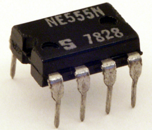
555 Timer IC
The IC 555 timer was invented by “Signetic Corporation” and it was termed as SE or NE555 timer. Generally, it is a monolithic timing circuit that gives precise and highly stable delays of time or oscillation. These types of ICs are very cheap and reliable in cost when we compared with the OP-Amp applications in the same areas. These ICs are used as an astable and monostable multivibrators in digital logic probes, DC-DC converters, tachometers, analog frequency meters, voltage regulators, temperature controlled and measurement devices. The IC SE555 is used for where the temperature ranges from – 55°C to 125°C and the IC NE555 is used for where the temperature ranges from 0° to 70°C.
What is a 555 Timer IC?
The IC 555 timer is a one type of chip used in different applications like an oscillator, pulse generation, timer. The designing of IC 555 timers can be done by using various electrical and electronic components like transistors, resistors, diodes and a flip flop. The operating range of this IC ranges from 4.5V -15V DC supply. The functional parts of the 555 timer IC include flip-flop, voltage divider and a comparator. The main function of this IC is to generate an accurate timing pulse. In the monostable mode, the delay of this IC is controlled by the external components like a resistor and capacitor. In the astable mode, both the duty cycle & frequency are controlled by two external resistors and one capacitor.
555 Timer IC Pin Configuration
The 555 timer IC consist of 8-pins where each pin has some function. The pin configuration of this IC is shown below.
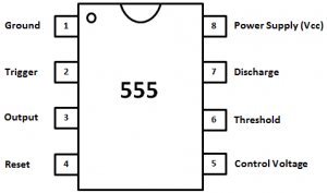
Pin Configuration of 555 Timer IC
GND Pin
Pin-1 is a GND pin which is used to supply a zero voltage to the IC.
Trigger Pin
Pin-2 is a trigger pin which is used to convert the FF from set to RST (reset). The output of the timer depends on the amplitude of the external trigger pulse that is applied to the trigger pin.
Output Pin
Pin-3 is an output pin.
Reset Pin
Pin-4 is a RST pin. When the negative pulse is applied to this pin to disable or reset, and false triggering can be neglected by connecting to VCC.
Control Voltage Pin
Pin-5 is the control voltage pin used to control the pulse width of the output waveform and also the levels of threshold and trigger. When an external voltage is applied to this pin, then the output waveform will be modulated
Threshold Pin
Pin-6 is the threshold pin, when the voltage is applied to threshold pin, then it contrasts with a reference voltage. The set state of the FF can be depends on the amplitude of this pin.
Discharge Pin
Pin-7 is the discharge pin, when the output of the open collector discharges a capacitor between the intervals, then it toggles the output from high to low.
Supply Terminal
Pin-8 is the voltage supply pin which is used to supply the voltage to the IC with respect to the ground terminal.
Operating Modes of 555 Timer IC
The operating modes of a 555 timer are astable, bistable and monostable. Each mode of operation signifies with a circuit diagram and its output.
Astable Mode Operation
In this mode, the circuit of the IC 555 timer produces the continuous pulses with exact frequency based on the value of the two resistors and capacitors. Here the charging and discharging of the capacitors depends on a specific voltage. The circuit diagram of the 555 timer in astable mode is shown below. If the voltage is applied to the below circuit, the capacitors continuously gets charged through two resistors and generates pulses continuously. In the following circuit pins 2 & 6 are shorted together for endless re-activate the circuit. If the o/p trigger pulse is high, then capacitor in the circuit totally discharges. Long time delays are accomplished by using the higher values of the resistors and capacitors.
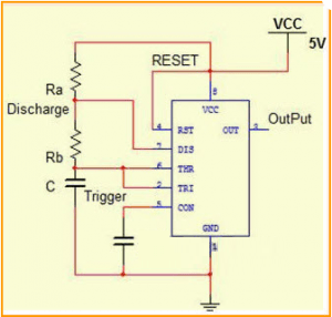
Astable Mode
Monostable Mode Operation
In this mode, the circuit generates only single pulse when the timer gets an indication from i/p of the trigger button. Pulse duration can be depends on the values of the resistor and capacitor If an activating pulse is applied to the i/p of the circuit through a push button, then the capacitor gets charge and the timer circuit extends a high pulse, then it remains high until capacitor totally discharges. If it is necessary to enhance the time delay, then higher rate of capacitor and resistor are required.
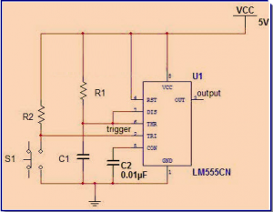
Monostable Mode
Bistable Mode Operation
In this mode, the circuit produces 2-stable state signals which are low and states. The o/p signals of low and high state signals are controlled by reset & activate the i/p pins, not by the charging & discharging of capacitors. If a low logic signal is given to active pin, then the o/p of the IC circuit goes to high level. If the low logic signal is given to the RST pin, then the o/p of the circuit goes to low level.
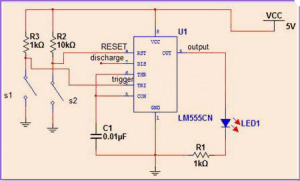
Bistable Mode
Important Features of the 555 Timer
- 555 timer IC works from a wide range of power supplies ranging from +5V to +18V.
- Sourcing or sinking load current is 200mA.
- The external components must be selected correctly, so that the timing intervals can be completed in several minutes along with the frequencies beyond several hundred kHz.
- The o/p of a 555 timer IC can drive TTl due to its high current o/p.
- It takes a temperature stability of 50 ppm/oC change in temperature (ppm means parts per million)
- The timer’s duty cycle is adjustable.
- The max power dissipation per package is 600 milliwatts & its reset and trigger i/ps has logic compatibility.
555 Timer Circuits
The 555 timer ICs are used to generate a precise square wave form and that is used in many circuits. This circuit is designed with transistors, diodes, resistors and flip flops, and this circuit can be worked in the range of 4.5-15V DC supply. The 555 timer circuit consists of three functional parts, namely flip-flops, a comparator and a voltage divider.
The main function of the comparator is to compare 2-i/p voltage levels such as inverting (-) and non-inverting (+) terminals. If the ‘V’ is high at the non inverting terminal, then the o/p is high. The /p resistance of perfect comparator is infinite.
As the i/p resistance is endless in the comparator, the voltage between all the 3-resistors are similarly divided and the value across each resistor is Vin/3
Flip/flops are digital electronic devices and it has a memory. If the i/p is high while low at R, then the o/p at Q is high. When S is high, o/p of the Q is also high & if R is high, then the o/p of the Q is low.
555 Timer IC based Projects for Engineering Students
The 555 timer IC is used in many electronic engineering projects to generate a pulse signal. Here we have discussed some major 555 timer IC based projects and these are very useful for engineering students.
Low-High Voltage DC Converter using IC 555
This project is used to develop the voltage nearly double to the i/p voltage using the voltage multiplier principle. For example, If the input voltage is around 5V DC, then the o/p we can get is around 10V DC. This project is designed with 555 timer, it operates in astable mode. In this project, the capacitors are connected in series and to charge these capacitors IC 555 timer delivers the clock pulses. This charged capacitors change the voltage which is nearly equal to the double the i/p voltage. The o/p can be calculated by using the multimeter.
Wire Loop Breaking Alarm Signal for Burglars
This project is used to identify when the thief attacks to break the window glass act to give an alarm. This project is designed with a 555 timer IC and this project is used as a security system. When the wire loop breaks, then the IC activates the buzzer to give an alert for indication.
Hidden Active Cell Phone Detector
This project is designed to identify any activated mobile phone from one and half feet distance to avoid the use of unauthorized cell phone in prohibited areas or defense security. This project is designed with 555 timer IC which operates in monostable mode. When any unknown person tries to make a call then the buzzer will give a signal presence of an active cell phone.
Touch Controlled Load Switch
This project is designed to regulate a load for the short time duration by using a touch sensitive switch and a 555 timer IC. This IC operates in monostable mode and activates by a touch plate that is connected to its trigger pin. The o/p of the IC provides logic high for a fixed time interval which is decided by the RC time constant. The o/p makes a relay to switch ON the load for that duration after that it switches OFF automatically.
Please refer to this link to know more about Distance Relay.
Please refer to this link for 555 IC Timer MCQs
Thus, this is all about 555 timer IC basics, pin description and operating modes. We hope that you have got a better understanding of this concept . Furthermore¸any queries regarding this concept or engineering project ideas, please give your valuable suggestions by commenting in the comment section below. Here is a question for you, what is the main function of a 555 timer IC?