The JIS semiconductor designation transistors in Japan start with a 2S prefix however sometimes this prefix is not noticeable on the package. So it might be listed as simply without prefix by a supplier. Sometimes this series has suffixes like O, R & BL, which stand for orange, red, and blue which indicate variants like tighter hFE groupings. 2SA PNP or 2SC NPN transistors indicate high-frequency type transistors, 2SB PNP or 2SD NPN series transistors indicate low-frequency type and 2SJ or 2SK series indicates P-channel and N-channel FETs. This article briefly explains 2SA series transistors like the 2SC3358 transistor, used for TV circuits and audio amplifiers.
What is a 2SC3358 Transistor?
The 2SC3358 is NPN silicon epitaxial planar type BJT, commonly used in different applications wherever high-frequency characteristics and low noise are necessary like in amplifier applications. This transistor has high voltage & high-speed switching, high current gain, and low CE saturation voltage.
2SC3358 transistor is used in high voltage switching applications like DC-DC converters and audio frequency power amplifiers. While designing any amplifier circuit using a 2SC3358 transistor, it is significant to consider these parameters like; its transition frequency, voltage or current ratings, and noise figure to make sure best performance.
While looking for a suitable transistor for your application based on a few factors, it is very important to look into a few points on How to Select a Transistor.
2SC3358 Transistor Pin Configuration:
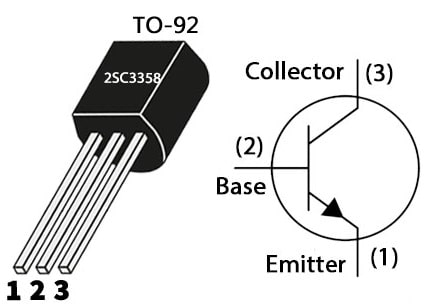
2SC3358 transistor pin configuration is shown below. This transistor includes three pins which carry electrical current & help in making a connection to an external circuit. Here each pin of this transistor and its functionality are explained below.

2SC3358 Transistor Pin Configuration
- Pin-1 (Emitter): The emitter terminal is also called the negative lead of the transistor and is indicated with the letter ‘E’. This terminal is heavily doped and moderately sized. Its main function is to supply the majority of carriers by supporting the electricity flow.
- Pin-2 (Base): This terminal helps in activating the transistor and is indicated with a ‘B’ letter. It is the middle terminal of the emitter & the collector. The base terminal is thin & lightly doped, so its main function is to supply the charge carriers from the emitter terminal to the collector.
- Pin-3 (Collector): The collector terminal is the positive lead which is indicated with a ‘C’ letter. It collects charge carriers emitted by the emitter terminal through the base terminal. This terminal is larger and moderately doped as compared to both the base & emitter terminals.
Features & Specifications
The features and specifications of the 2SC3358 transistor include the following.
- It is a silicon epitaxial planar transistor.
- This transistor has three terminals.
- It is made with Si material.
- Its polarity is NPN.
- This transistor has high gain and less noise.
- It is available in the TO131 package.
- Its collector power dissipation maximum or Pc is 0.3 Watts.
- Collector to base voltage or Vcb maximum is 20 Volts.
- The Max collector current or Ic is 0.1A.
- Its transition frequency or ft is 7000 MHz.
- The minimum forward current transfer ratio or hFE is 20.
- Its operating junction temperature or Tj maximum is 125 °C
Equivalent & Replacement Transistors
Equivalent 2SC3358 transistors are; 2SC3353, 2SC3355, 2SC3354, 2SC3356, 2SC3358, 2SC3357, 2SC3359, TIP31C, 2SC336, 2SC3361, 2SC3361S5, 2SC3361S6, 2SC3361S4, 2SC3363, 2SC3364, 2SC3362 and 2SC3365. 2SC3358 transistor can be replaced with a BFG195 transistor.
Replacing a suitable transistor in any circuit based on requirement is very important. To know how to replace it, please refer to this; Replacing Transistors in Electronic Circuits: Factors and Considerations.
UHF Antenna Booster Circuit
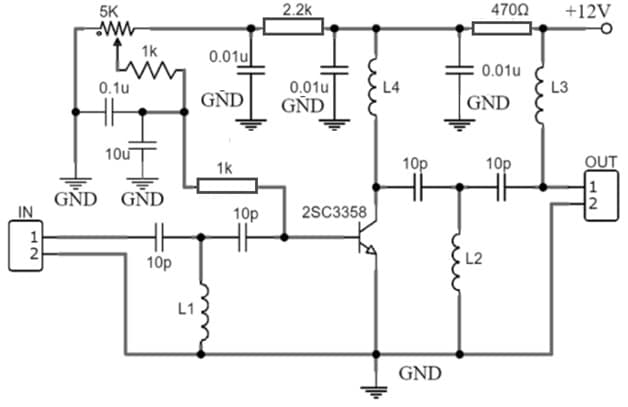
Generally, an antenna amplifier or booster in electronics is a device used to improve an antenna signal normally into an output by related impedance like the input impedance. The amplifier amplifies everything like both the noise and ideal sign available at the antenna. In this circuit, 300 ohms for the twin-lead cable and a 75-ohm for the coaxial cable. Here, you need to maintain all the parts leads as short to get the best outcomes place the circuit within a waterproof case, and set up it near the radio wire.
The required components to make this UHA antenna amplifier circuit mainly include; a 2SC3358 transistor, Coil 2 turns, 10 Turns, 5K variable resistor, 1K, 470Ω and 2.2K resistors, 0.01µF, 10pF & 10µF capacitors and 12V Battery. Connect this circuit as per the amplifier circuit shown below.

UHF Antenna Booster Circuit
Working
This UHF radio wire amplifier or booster circuit is used to amplify the UHF band signals which ranges from 400 MHz – 850 MHz. This UHF antenna booster circuit uses a single transistor only and provides 15dB amplification. In the circuit, both the L1 & L2 are equivalent to 0.5mm 2 turns of enameled copper wire which wounded on 3mm former, so these two coils are air core. Both L3 & L4 are equal to 10uH HF choke (or) 0.2mm ten turns above the ferrite core.
This circuit’s current usage ranges from 5 mA to 15 mA. A choke loop is used to control the circuit thus it will keep the DC voltage from going into the TV. A UHF antenna amplifier simply supports a radio signal widely for gadgets that obtain radio waves. Many devices contain an RF amplifier stage within their circuit that improves the antenna signal. These are used in TVs, radios, Wi-Fi, Bluetooth devices & cell phones to amplify everything.
Connecting a base resistor to the base terminal of the transistor is mandatory to avoid it being damaged. So, Please refer to this link for; Choosing Base Resistance for Transistors in Electronic Circuits.
RF Mobile Signal Detector Circuit
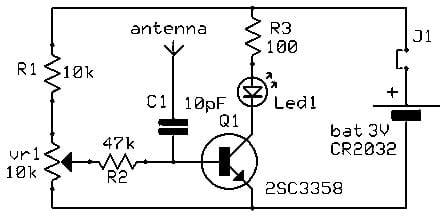
A simple RF mobile signal detector or RF sniffer circuit diagram is shown below which is used to identify VHF or UHF 4G LTE.
The required components to make this mobile signal detector circuit mainly include; resistors like; 100 Ohm, 10 KOhm, and 47 KOhm, variable resistor 10 KOhm, 2SC3358 transistor, Blue LED, ceramic capacitor – 10 pF, Antenna -10 Cm and 3V CR2032 battery. Connect this simple circuit as per the diagram shown below.

RF Mobile Signal Detector with 2SC3358 Transistor
Working
The 2SC3358 Transistor in this circuit is a high-gain transistor mainly designed to operate at up to 7GHz frequencies. The J1 jumper is the power switch and the vr1 Potentiometer is used to set the Q1 transistor’s bias voltage. So it must be calibrated for the least LED brightness without an RF radiation source near to antenna. Here, a 10cm wire antenna receives electromagnetic waves, and a 10 pF capacitor simply blocks low frequencies.
This is a simple RF mobile signal detector circuit that is driven through a high-frequency-based RF transistor equal to 6GHz. This circuit easily detects low as well as high-frequency-based RF and electromagnetic signals. So, in this demonstration, a smartphone with 4G LTE is used. Whenever the internet is working then the signal will be captured thus, the LED will light up. One more test is performed on an antenna that transmits a 20 Mhz signal & it lights up LED very brightly due to the 5 Volt power being used to amplify the 4G modem.
Whenever the phone gets a 4G signal from the internet, SMS or calling, etc, this circuit will get the signal & amplify via the RF transistor. After that, the amplification result will be shown on the blinking LED. When the signal is brighter then the LED will be brighter otherwise it will be dimmer.
The VR1 variable resistor in this circuit controls how much current should be supplied so that the LED in this circuit can glow. So, if too much current is supplied then the LED will constantly glow even if there is no signal. So you have to change to the point where it simply gets minimal current from the battery & when it is included with the signal detected then the LED will blink.
Advantages & Disadvantages
The advantages of the 2SC3358 transistor include the following.
- The 2SC3358 is a very efficient and reliable transistor that can be utilized in different electronic devices.
- These are not expensive to manufacture.
- It is an ideal choice mainly for low-power applications due to low collector-emitter voltage and high collector current.
- These are available in smaller sizes, use low power, and have longer life spans.
- Its testing with a multimeter is easy.
- It can switch easily between the ON state to bear large currents while equally blocking extremely high voltages whenever in the OFF state.
- It is capable of operating at 10 to 15 KHz switching frequencies.
- The low operational voltage of this transistor will make it secure and appropriate to fit into fixed spaces.
- It has a simple & strong design.
- It works very well in cool temperatures and, thus doesn’t need a heating element whereas output voltage remains stable whenever temperatures increase or drop.
The disadvantages of the 2SC3358 transistor include the following.
- This transistor is very responsive to temperature.
- It generates heat.
- A transistor can be damaged because of the second breakdown or thermal runaway.
- It has a very low reverse-blocking capacity.
- The o/p voltage cannot be easily changed because the DC o/p voltage cannot be modifiable.
- Transistor has less thermal stability, are most effective through radiation, have low switching frequency, have very complex control, etc.
- It produces more noise.
2SC3358 Transistor Applications
The 2SC3358 is a frequently used NPN-type bipolar junction transistor that is well known because of its low noise performance and high frequency. This transistor is used normally in applications wherever high frequency and low noise characteristics are necessary. Some of the 2SC3358 transistor applications include the following.
Signal Processing Circuits
This transistor is used in signal processing tasks wherever low noise & high frequency are significant like; PLLs, frequency modulators, RF signal processing applications, etc.
Oscillators
This transistor is perfect for oscillator circuits due to high-frequency abilities like frequency synthesizers & local oscillators utilized in a variety of communication applications.
RF Amplifiers
The 2SC3358 transistor is appropriate for (RF amplifier stages within communication devices because of its higher frequency performance; like; RF preamplifiers, RF signal boosters & VHF/UHF radios.
Buffer Stages
The 2SC3358 transistor can be utilized as a buffer amplifier to separate different circuit stages while keeping signal integrity, particularly within high-frequency signal chains.
Mixers and Multipliers
This transistor is used within mixer circuits wherever signals are changed or united from one frequency to another frequency and is common within microwave & RF communication systems.
Switching Circuits
This transistor is normally used within analog applications and also in high-speed switching circuits wherever quick response times are serious.
LNAs (Low Noise Amplifiers)
This transistor is appropriate to use within the primary phase of low-noise amplifiers due to its low-noise characteristics, mainly in sensitivity-critical applications such as radio telescopes and satellite receivers.
- 2SC3358 is a RF BJT, utilized in separate semiconductor products.
- This is a suitable transistor for high-frequency applications.
- It can be utilized in RF amplifiers, mixers, and oscillators.
Please refer to this link for the 2SC3358 Transistor Datasheet.
Thus, this is an overview of the 2SC3358 transistor, pinout, specifications, circuit, working, and its applications. This is an NPN silicon epitaxial transistor mainly designed for LNA (low noise amplifier) at different bands like; VHF, CATV & UHF. This transistor has dynamic range as well as good current. Here is a question for you, what is 2SC3353 transistor?